Forum rules
The DIY forum is for personal projects (things that are not for sale, not in production), info sharing, peer to peer assistance. No backdoor spamming (DIY posts that are actually advertisements for your business). No clones of in-production pedals. If you have concerns or questions, feel free to PM admin. Thanks so much!
crochambeau wrote:Yeah, I wouldn't bend over backwards to integrate mounting points if it's not a popular practice. I've got a solution that doesn't involved drilling the board, rip a profile on some scrap wood with the table saw and suspend the board between those points.
I would just board mount 1 pot for enclosure mounting and keep the rest as flying. Keeps it simple.
multi_s wrote:looks like lots of space for some drill holes but also you could just mount 2 or 3 of the pots or switches on the board and the rest off board, still allowing for huge knobs etc.
I appreciate everyone's input, like I said to eatyourguitar: no reason to change the design based on any requests I have - unless of course it's a design suggestion that would benefit others.
Since it's come up a couple times now I'll just flat out state that I don't mount PCBs off panel controls. Having over the years repaired stress fractures on a variety of such devices that saw rough use it's one assembly method I no longer employ. I know it can be done in a robust manner, it's just my choice to build otherwise.
crochambeau wrote:
I appreciate everyone's input, like I said to eatyourguitar: no reason to change the design based on any requests I have - unless of course it's a design suggestion that would benefit others.
Since it's come up a couple times now I'll just flat out state that I don't mount PCBs off panel controls. Having over the years repaired stress fractures on a variety of such devices that saw rough use it's one assembly method I no longer employ. I know it can be done in a robust manner, it's just my choice to build otherwise.
I don;t know if you are familiar with eagle but its literally 4 mouse clicks to add 3 holes.pretty easy for an expert like the op i'd wager.
Ben79 wrote:Would it make sense for the pads for the germs to be set in a line so cheap inline sockets can be easily soldered in there?
Best of both worlds:
What program are you using? If you can import .mod modules from Kicad I'd be happy to share a footprint (honestly it seems the least I can do for the inclusion to this kickass project).
EDIT: here's one that lines up with standard SIP offset, which is what I use for "cheap" BJT sockets, but it does have kicad in the extension, hopefully it's a somewhat standard format that can translate to other platforms..
eagle uses some sort of .xml files for pretty much everything, so converting shouldn't be that bad, but i don't think there is a converter to go from kicad to eagle at the moment (but the opposite exists). You could just draw that footprint in eagle though. The easiest would be just opening the library with the current part and creating a new footprint/package with the spacing croch drew. then open the current part and add a package variant that uses the new pads you just drew. IIRC you have to use "append" or something like that to get 2 pads to share the same signal. Then you should be able to just use the replace command and swap the new package without cutting any nets etc.
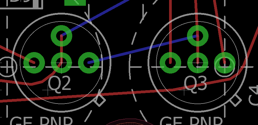
I can create a part but I did not want to. I opened the part to check the drill size for the TO-5. then I made two vias on the PCB. I renamed the vias to the net names of the bases, n$5 and n$1 respectively. I ripped up and routed very easy fix.
If you used a via I would do some double checking because they don't usually have exposed area in the solder mask. ie a via is not the same as a pad. It will depend on your dru and the cam setup. I think the solder mask layers in eagle are tCream and bCream. You could type "display tcream bcream" in the command line to display and verify whether or not the copper in the vias you added is actually exposed and i would double check any gerbers afterwards. If they are not exposed you will have a hard time to solder a through hole part to the via. just a heads up.
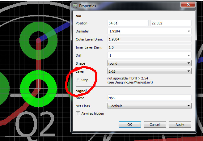
I will check the gerbers in another program. maybe you can help. should this stop box beck checked? I'm pretty sure its ok this is default and they are always exposed IIRC.
Is the stop command aimed at solder mask? I've never come across it in my travels. I would think you'll see any irregularities when you view it on another gerber program (and if the manufacturer does preview all the better).
ok multi_s is %100 correct about the solder mask. I need to actually check the box to get what I want. however, tcream is for SMD stencil. if you make visible in eagle the Tstop you will see the problem immediately. if you are keeping score that is all of two major flaws in this circuit and PCB have been corrected by the wonderful multi_s.
ah ok tstop. sorry i was not on a computer with eagle to double check the layers when I was responding.
usually for checking gerbers i just use this online viewer because i can;t find a simple free one that works on windows (maybe you know one?). You can compress your gerbers into a .zip then upload all the layers at once. it seems to work ok.
on windows or linux use gerbv. I use gerbv to delete things from the silkscreen layer by hand. for example the pot outline can obfuscate the text so I *delete* that shit.
eatyourguitar wrote:on windows or linux use gerbv. I use gerbv to delete things from the silkscreen layer by hand. for example the pot outline can obfuscate the text so I *delete* that shit.
cool i will check it out later today. i didn't actually realize that it would build on windows.
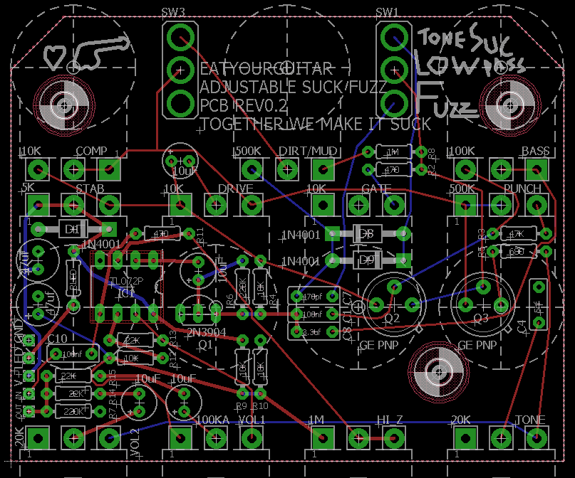
i was going to mention re the text that it could be cleaned up, ie sw1 and sw2 designators aren't even on the pcb etc, but just assumed you had not got around to that part yet. (:


Keeps it simple.